Telecommunications
Communication infrastructure (Base Stations)
-
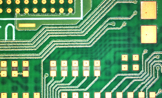
High Layer Count PCB
The technology of high alignment accuracy as well as applying multi-stacked HDI technology, the high density multi-layer structure is tailored for customers requirements.
-
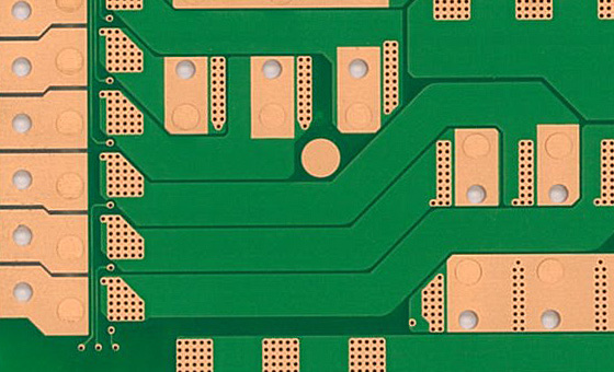
Heavy Copper PCB
Carries various types of copper PCBs (with up to 200 μm copper thickness) used for large electric current units that can support regular electric current over 50A.
-
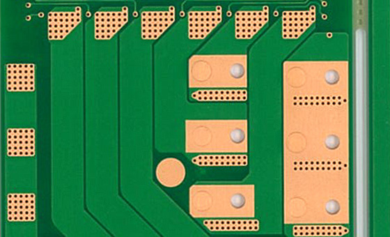
Copper Inlay PCB
Copper inlay PCB can release heat from heater elements mounted on an electronic circuit board through copper inlays to a bottom side heat sink.
-
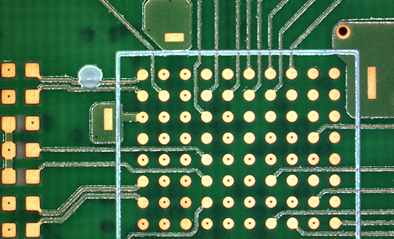
HDI PCB (M-VIA Ⅰ/Ⅱ)
HDI PCB is composed of Staggered Via and Stacked Vias. Laser Via hole, IVH and Plated Through Hole are used in combination.
-
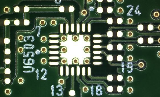
Double-sided/Multi-Layer PCB
Multi-layer through-hole PCB is used for a wide variety of applications from special products to general usage.