


Embedded Device PCBs
A board for flexible wiring and ultra-compactness. As the number of passive components mounted on small mobile devices increases, there is a demand for higher density component mounting. However, as there is a limit to the surface mounting area that can be achieved with conventional surface mounting technology (two-dimensional mounting arrangement), three-dimensional mounting arrangement using "component-embedded boards" has been proposed. Meiko has been researching and developing "component-embedded boards" for many years and has an excellent track record.
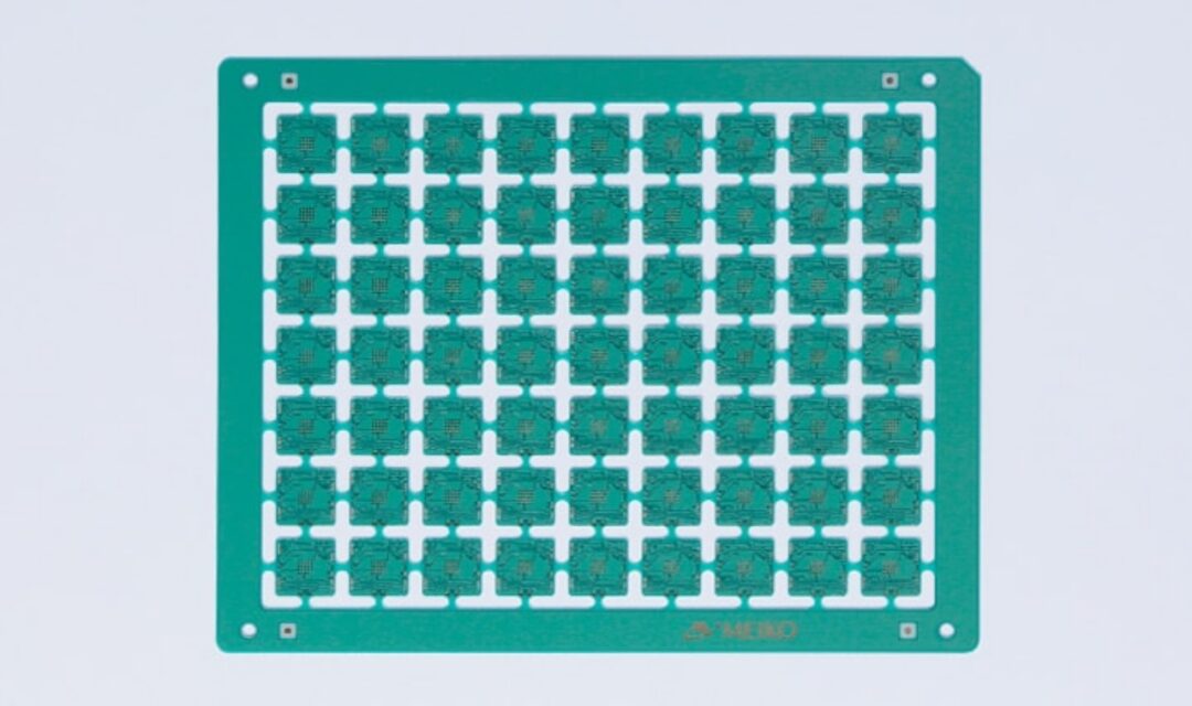
Features of Embedded Device PCBss
- Miniaturization and high integration of products that mount chip components inside a substrate
- Reduced wiring length reduces inductance and noise
Main uses
-
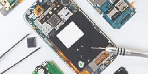
Communication Module
-

Wearable devices
-
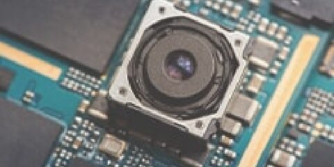
Camera module
Contact About the productInquiry
In addition to major corporate clients, we also serve universities, research institutes,
We also accept consultations from venture companies.
We also accept one-off orders from design companies and parts trading companies,
Please feel free to contact us for technical advice.

