Industrial equipment
Medical equipment
-
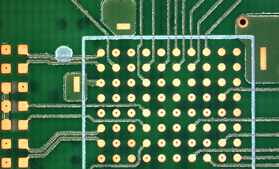
HDI PCB (M-VIA Ⅰ/Ⅱ)
HDI PCB is composed of Staggered Via and Stacked Vias. Laser Via hole, IVH and Plated Through Hole are used in combination.
-
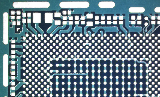
AnyLayer PCB (M-VIA Ⅲ)
AnyLayer PCB with Laser Via and Filled Plating on each layer, it is possible to build thin construction and 0.4mm pitch CSP by AnyLayer interconnection.
-
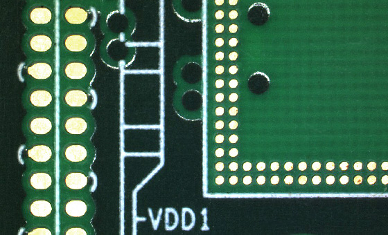
Embedded Devices PCB
Meiko has been developing a connection process using laser via and plating in addition to a bonding process using solder materials.
-
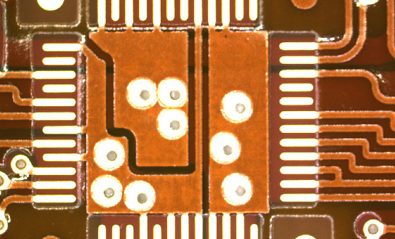
FPC
FPC (flexible printed circuits) is also known as a flexible PCB. It is excellent thinness, lightness, softness and durability using insulating film as a material.
-
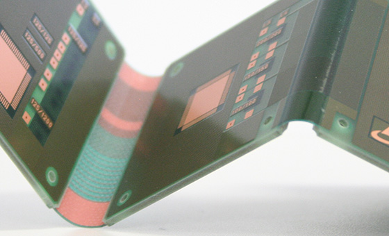
FR4-FLEX/M-VIA Flex®
FR4-FLEX/M-VIA Flex® is rigid-flex PCB without polyimide that can be utilized for applications that do not require repeated bending and as an alternative to connectors.
-
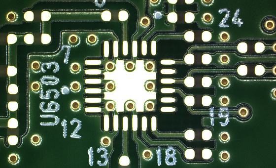
Double-sided/Multi-Layer PCB
Multi-layer through-hole PCB is used for a wide variety of applications from special products to general usage.